
In the fast-paced world of electronics, speed is everything. That’s where rapid PCB prototyping comes into play. It’s not just about getting a product to market quickly, but also about testing and refining designs in a flash. This guide will illuminate the ins and outs of this vital service.
From understanding the basics to exploring advanced techniques, we’ll delve into every aspect of rapid PCB prototyping. Whether you’re a seasoned engineer or a newbie in the electronics industry, this guide promises to be your ultimate companion. So, strap in and prepare to accelerate your design process like never before.
Stay tuned as we unravel the mystery of rapid PCB prototyping service, helping you navigate its complexities with ease and confidence. This is more than just a guide; it’s your roadmap to faster, more efficient electronics design.
Understanding Rapid PCB Prototyping
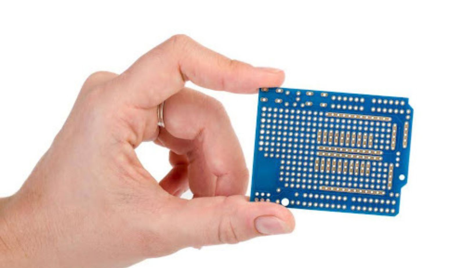
Rapid PCB prototyping, in essence, serves to expedite the creation of circuit board prototypes. This fast-paced service is the pinnacle of innovation in the expansive field of electronics.
The Importance of Rapid PCB Prototyping
Speed is definitely not a term to underestimate in the realm of PCB Prototyping Service and PCB Standard Production. Let’s delve into why it’s so crucial. First off, quick prototyping paves the way to proof-of-concepts that are immediate and substantial.
In rapid PCB prototyping, a delay in testing is not a worry, allowing for quick iterations and an accelerated Time-to-Market. In addition, getting PCB prototypes from service providers like WellPCB means you’ll have your design in hand faster, allowing for early detection and rectification of design flaws.
The Process of Rapid PCB Prototyping
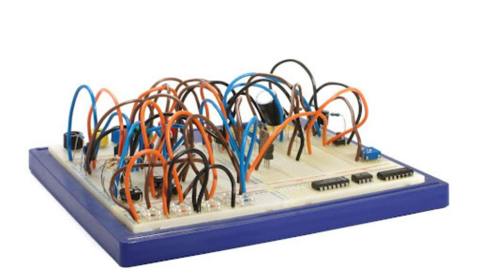
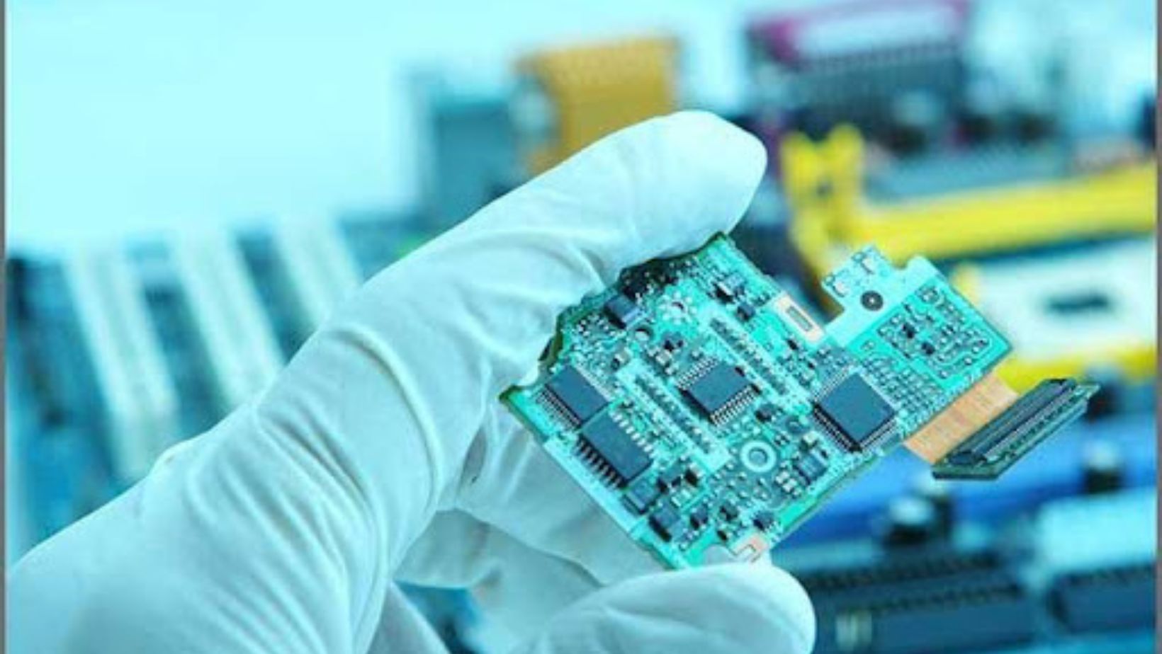
Unfolding the process of rapid PCB prototyping can provide insightful depth, aiding in navigating its intricacies. The journey kicks off with the design stage, where the PCB layout is conceived and evaluated digitally. Then comes the prototyping phase, where it brings the design to life, either as a single layer, multiple layers or as a complex through-hole structure. The final stage – testing and evaluation. This phase ensures that the prototype operates as intended, free of misconnections or short circuits. Post this phase, a transition to large scale PCB manufacturing may ensue if the design meets the requirements. Needless to say, each stage requires meticulous attention to detail to ensure the ensuing PCB lives up to its purpose.
Choosing the Right Rapid PCB Prototyping Service
With the role of rapid PCB prototyping in product development established, choosing the right service becomes vital.
Considerations When Selecting a Provider
Selecting a Rapid PCB Prototyping Service demands critical analysis. Here’s a distilled list of key considerations:
- Time-to-Market: Go for services that expedite Time-to-Market. This helps in faster iterations and quicker product development.
- Capability: Assess if the provider can handle projects of different complexity, including multiple layers and through-hole PCB.
- Standard Production: Ensure the provider offers both PCB Prototyping Service and PCB Standard Production. Prototype completion is just the initial step, and the ability to seamlessly transition to mass production is crucial.
- Service Inclusion: Opt for service providers who facilitate both PCB manufacturing and assembly under one roof. Integrated services can increase efficiency and reduce overall project timeline.
- Proof-of-concepts: Lastly, watch for providers that offer proof-of-concepts. This can assist in validating the applicability of the prototype in the early stages, saving costs down the line.
One example is WellPCB, who consistently delivers in these areas and has built a reputation for quality and reliable services in rapid PCB prototyping.
Potential Challenges and How to Overcome Them
Every journey has its bumps, and opting for rapid PCB prototyping is no exception. Here are some potential challenges:
- Design Issues: Incorrect design inputs can result in faulty PCB prototypes. To overcome this, make use of advanced design software and testing tools in the pre-production phase.
- Cost Overruns: Rapid prototyping, although efficient, can lead to increased costs if not managed well. Keeping a thorough track of resource utilization and adopting cost-efficient methodologies is crucial.
- Time Delays: Delays in prototype production can occur due to unforeseen challenges. Thus, opting for a reliable PCB Prototyping Service with a proven track record of on-time delivery is essential.
- Quality Concerns: Compromised quality can derail product development. Make sure to choose a service provider who upholds rigorous quality standards throughout the process.
It’s essential to anticipate these challenges as they can influence the decision in choosing the right PCB prototyping service provider.
Tips to Optimize Your PCB Design for Rapid Prototyping
Building on the discussion about the vital role of rapid PCB prototyping in product development, this section unfolds ways to optimize your PCB design. This includes selecting the right design software and inventing strategies to reduce errors.
Design Software Recommendations
Keeping in view the criticality of perfect PCB design in the rapid prototyping process, choosing suitable design software becomes an essential step. Design software like Altium Designer, Eagle, and OrCad proves to be excellent choices considering their features conducive to effective prototyping.
Eagle, known for its user-friendly interface and popular schematics editor, is generally preferred by hobbyists and small-scale industries. Altium Designer, with advanced features like real-time cost estimation and obstacle subdivision, finds its place among professionals in larger companies.
Finally, OrCad, famous for its scalable solutions, assists in configuring the software to its optimal settings. This inventiveness enhances the quality of PCB Prototyping Service and PCB Standard Production, making it favorable for manufacturers.
Design Tips to Reduce Errors
In reducing errors in the PCB design for rapid prototyping, a few tips come in handy. Firstly, it’s best to avoid complex layouts. Remember, simple layouts can have an equally high performance.

It’s also advisable to stick with the through-hole technique for PCB manufacturing until there’s a solidity of understanding in working with surface-mount technology. Numerous errors could be avoided by simply organising and verifying the schematics regularly.
Finally, considering multiple layers during the design phase proves essential when dealing with high-speed circuits or small form factors. It’s preferable to incorporate proof-of-concepts in the design process, ensuring that the functional aspects of the design have been verified. Reliable service providers such as WellPCB can significantly assist in implementing these methods, enhancing Time-to-Market and product quality.
Case Study: Successful Rapid PCB Prototyping in Practice
This case study serves to illustrate how the insights discussed in the previous sections apply to a real-life scenario in the use of a rapid PCB prototyping service.
Project Background and Goals
In this instance, the client wished to bring a cutting-edge device to market. To reach this goal, the client utilized a reputable rapid PCB prototyping service from WellPCB, aiming to refine the product through numerous iterative prototypes before transitioning to mass production, thus optimizing Time-to-Market.
The project specifics were as follows: the device required a PCB design capable of handling multiple layers. Challenges inherent in this complexity included ensuring the desired design would translate effectively into actual hardware and maintaining form and function through the various stages of PCB prototyping.
Going Through the Prototyping Stages
In this case, the client began with a simple, single-layer PCB for assessing the initial concept. Following this, they underwent several stages of prototyping. First, a double-layer PCB was constructed to test the feasibility of adding more complexity. Each successful test enabled further enhancements, with prototypes evolving through multiple layers, testing both service provider for assembly, and the team’s expertise ensured the project’s success.
As a result of investing in a dedicated PCB prototyping phase, the client was able to identify potential issues before moving to the pricier PCB standard production stage. It’s clear, therefore, that strategic use of rapid PCB prototyping services can be a game-changer, especially when the goal is innovation without compromising Time-to-Market.
This case study illustrates how keeping prototypes simple, gradually adding complexity, and relying on trustworthy service providers like WellPCB can lead to success in the competitive electronics market.
Evaluating the Cost of Rapid PCB Prototyping Service
Finances play a pivotal role in deciding the path of prototyping. A thorough understanding of cost factors and budget-friendly strategies aids in leveraging the benefits of Rapid PCB Prototyping Services efficiently.
The Factors Affecting PCB Prototyping Cost
There’s an assortment of variables that impact the cost of PCB Prototyping Services. Firstly, PCB’s complexity escalates the expenses.
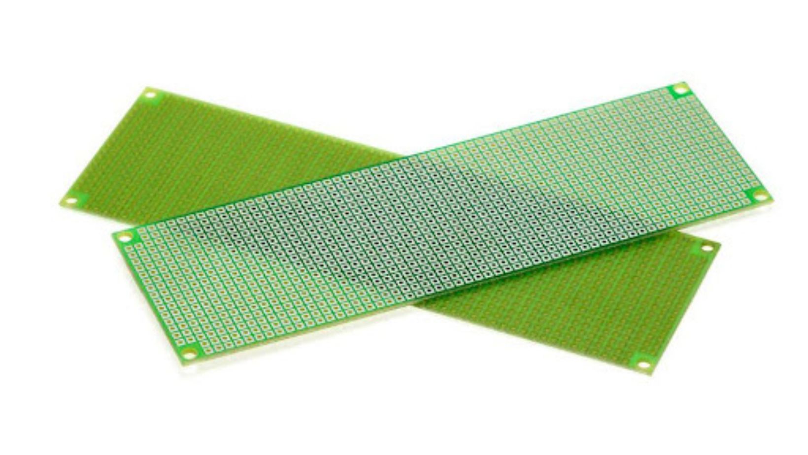
The count of layers, whether single or multiple layers, influences the manufacturing process, thereby increasing costs.
The prototyping method, too, plays a crucial role, with PCB Standard Production being costlier than proof-of-concepts or small-scale prototypes. Material selection also affects the price, with certain materials like high-speed laminates incurring higher charges.
The location of the service provider for assembly can also significantly influence the final cost. Overseas providers may offer lower costs, but shipping expenses and possible communication barriers need consideration.
Finally, the cost factor also depends on technical specifications like the type of vias used. Normal vias, for example, are relatively cheap, but blind or buried vias, often required in compact designs, can bump up manufacturing costs due to the intricacies involved in crafting pathways through multiple layers. For instance, the cost of fabrication employing through-hole vias will differ vastly from that of surface mount technology.
Tips to Save Costs in PCB Prototyping
Minimizing PCB Prototyping costs without compromising on the reliability of the end-product is pivotal. Firstly, simplifying the design wherever feasible can lead to significant savings. Reducing the number of layers, or opting for standard PCB sizes can help downsize the expenses.
Next, ensuring efficient Communication with the service provider, particularly when they’re located overseas, can circumvent misunderstandings and costly errors. Make certain to accurately convey your design specifications and changes, to avoid pricey alterations occur post-production.
Moreover, investing some initial time and resources in designing and testing the PCB can lead to considerable savings in the long run. Using software like Altium Designer aids in identifying potential errors early. Take the case of WellPCB, which provided iterative prototypes. This stage-wise scrutiny and testing, though seemingly expensive at first, have been shown to optimize Time-to-Market and save enormous costs by preventing full-scale errors.
Selecting the right PCB prototypes and services, prudently making technical choices based on the complexity of the design, accurate communication, and diligent testing, can significantly reduce the overall prototyping cost.
Conclusion
Choosing rapid PCB prototyping can be a game changer for product development. It’s not just about speed, but also the quality and precision that can be achieved. It’s vital to pick the right service provider and use advanced software like Altium Designer to iron out any design issues. The case study with WellPCB demonstrated the power of iterative processes in optimizing Time-to-Market. When it comes to cost, remember that factors like PCB complexity, prototyping methods, materials, and location of the service provider play a role. But don’t fret – there are ways to save, such as simplifying designs and investing wisely in design and testing phases. In the end, strategic decision-making in choosing PCB prototypes and services can lead to reduced costs, reliable products, and a timely market entry. That’s the power of rapid PCB prototyping.